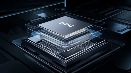
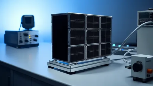
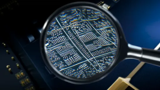
The semiconductor industry is undergoing a paradigm shift with the emergence of Data Processing Units (DPUs) as specialized accelerators for modern data-centric workloads. Unlike traditional CPUs and GPUs, DPUs are designed to offload and accelerate infrastructure tasks like networking, storage, and security, enabling more efficient data center operations. A virtual teardown of DPU architectures reveals fascinating insights into how these chips are redefining the boundaries of computational efficiency.
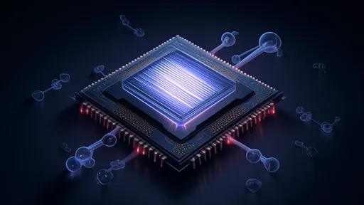
At the heart of every DPU lies a heterogeneous architecture that combines multiple processing elements tailored for specific functions. Arm-based multicore CPUs often serve as the control plane, managing orchestration and coordination tasks. These cores are complemented by high-performance packet processing engines that handle network traffic at line rates, typically implemented through custom hardware or programmable accelerators. The storage subsystem frequently incorporates dedicated encryption/decryption blocks and DMA engines to enable secure, low-latency data movement.
The most intriguing aspect of DPU design emerges in the network interface layer, where cutting-edge implementations integrate 100-400GbE controllers directly onto the die. This tight coupling of network functionality eliminates traditional bottlenecks associated with discrete NICs. Some architectures go further by implementing smart NIC capabilities through programmable pipelines that can parse, modify, and forward packets without CPU intervention. The inclusion of match-action engines and statistical multiplexers allows for sophisticated traffic management at wire speed.
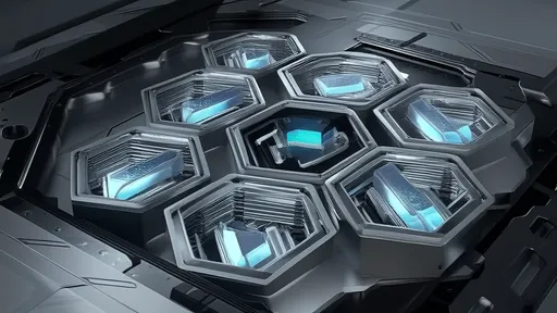
Memory subsystems in DPUs showcase equally innovative approaches. Most designs implement a multi-tiered memory hierarchy combining large DDR controllers for bulk data with low-latency SRAM or HBM for acceleration structures. The memory controllers often feature quality-of-service (QoS) mechanisms to prioritize critical traffic flows. Some architectures even incorporate near-memory processing elements that can perform basic operations directly in memory controllers, further reducing data movement.
Power efficiency has become a defining characteristic of DPU architectures. Through advanced power gating and dynamic voltage/frequency scaling, these chips maintain exceptional performance-per-watt metrics. The thermal design power (TDP) of most DPUs remains surprisingly low given their capabilities, typically ranging between 25-75W. This efficiency stems from the extensive use of domain-specific accelerators that avoid the overhead of general-purpose computation.
The software ecosystem surrounding DPUs reveals another layer of innovation. Unlike traditional processors that rely on standard operating systems, DPUs typically run lightweight real-time kernels or bare-metal applications tailored for specific workloads. The toolchains for these devices increasingly support high-level programming models that abstract the underlying hardware complexity, allowing developers to focus on functionality rather than low-level optimization.
Security features in DPU architectures have evolved to address modern threats. Most designs incorporate hardware root of trust modules, secure boot mechanisms, and memory encryption engines as standard features. Some implementations go further by including runtime attestation capabilities that continuously verify the integrity of both code and data. These security measures are particularly crucial as DPUs often handle sensitive infrastructure operations in multi-tenant environments.
Looking ahead, DPU architectures continue to evolve at a rapid pace. The next generation of designs promises even tighter integration of AI acceleration blocks for intelligent network processing and optical interface options for higher bandwidth connectivity. As hyperscalers and cloud providers increasingly adopt DPUs as standard infrastructure components, these specialized processors are poised to redefine data center economics and capabilities for years to come.
By /Jul 22, 2025

By /Jul 22, 2025
By /Jul 22, 2025

By /Jul 22, 2025

By /Jul 22, 2025

By /Jul 22, 2025

By /Jul 22, 2025
By /Jul 22, 2025

By /Jul 22, 2025

By /Jul 22, 2025
By /Jul 22, 2025
By /Jul 22, 2025

By /Jul 22, 2025
By /Jul 22, 2025

By /Jul 22, 2025
By /Jul 22, 2025

By /Jul 22, 2025

By /Jul 22, 2025