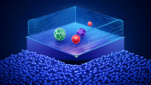
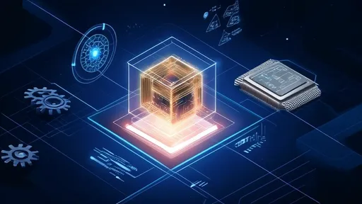
The semiconductor industry has long been dominated by silicon, but researchers may have finally discovered a material capable of dethroning the reigning champion. Borophene, an atomically thin 2D form of boron, is emerging as a revolutionary semiconductor material that could overcome the fundamental physical limits of silicon-based electronics.
Unlike graphene, which lacks an inherent bandgap, borophene exhibits tunable electronic properties that make it exceptionally promising for transistor applications. Recent breakthroughs in borophene synthesis and device fabrication have demonstrated electron mobility values surpassing silicon by nearly an order of magnitude, while maintaining excellent on/off current ratios essential for digital logic operations.
The Unique Properties of Borophene
What makes borophene particularly exciting is its anisotropic metallic character and intrinsic polymorphism. The material naturally forms different crystalline phases with varying arrangements of hexagonal holes in its atomic lattice. This structural flexibility allows researchers to "tune" borophene's electronic properties by controlling the phase during synthesis - a capability that simply doesn't exist with silicon.
Experimental measurements have shown that certain borophene phases exhibit carrier mobility exceeding 10,000 cm²/Vs at room temperature, compared to silicon's 1,400 cm²/Vs. Even more remarkably, theoretical calculations suggest that optimized borophene structures could reach mobility values above 100,000 cm²/Vs under ideal conditions.
Overcoming Silicon's Scaling Limits
As silicon transistors shrink below the 5nm node, engineers face increasingly difficult challenges with leakage currents, heat dissipation, and quantum tunneling effects. Borophene's atomic thinness (typically just one atomic layer thick) and excellent electrostatic control properties offer potential solutions to these scaling roadblocks.
Research teams at several leading universities have demonstrated borophene field-effect transistors (FETs) with channel lengths below 10nm that maintain excellent switching characteristics. These ultra-scaled devices show minimal short-channel effects that plague comparable silicon transistors, thanks to borophene's perfect 2D nature and lack of surface dangling bonds.
Manufacturing Challenges and Solutions
The path to borophene commercialization isn't without obstacles. The material's sensitivity to oxidation requires specialized handling under inert atmospheres or ultra-high vacuum conditions. However, recent advances in passivation techniques, including the development of protective capping layers, have significantly improved borophene's environmental stability.
Another challenge has been achieving uniform, large-area borophene growth. Early synthesis methods produced only micron-scale flakes, but newer chemical vapor deposition (CVD) approaches have demonstrated wafer-scale borophene films with acceptable uniformity. Researchers are optimistic that further refinements to these processes could make borophene compatible with existing semiconductor fabrication lines.
Beyond Conventional Transistors
Borophene's potential extends far beyond simply making better versions of existing transistor designs. Its unique properties enable entirely new device concepts that could revolutionize computing architectures. For instance, some borophene phases exhibit superconducting behavior at relatively high temperatures, opening possibilities for ultra-low-power superconducting electronics.
Another exciting direction involves exploiting borophene's mechanical flexibility for flexible and stretchable electronics applications. Unlike brittle silicon, borophene can withstand significant strain without degradation of its electronic properties, making it ideal for wearable devices and foldable displays.
The Road to Commercialization
While borophene transistors won't replace silicon chips tomorrow, the technology is progressing at an impressive pace. Several semiconductor giants have established borophene research programs, and prototype devices have already demonstrated performance metrics that meet or exceed industry roadmaps for future nodes.
Experts predict we may see the first commercial borophene-based devices within 5-7 years, likely initially appearing in specialized high-frequency or low-power applications where its advantages over silicon are most pronounced. Full-scale adoption in mainstream logic chips would require not just technological maturity but also the development of an entire ecosystem of design tools, manufacturing processes, and reliability standards.
A New Era of 2D Electronics
The emergence of borophene transistors represents more than just another material option - it signals a fundamental shift in how we approach semiconductor technology. For the first time, we have a material that combines the best attributes of 2D materials (atomic thinness, excellent electrostatics) with the electrical performance needed for practical high-speed electronics.
As research continues to unlock borophene's full potential, we may be witnessing the dawn of a post-silicon era in electronics. The coming years will be crucial in determining whether borophene can transition from laboratory curiosity to foundational technology that reshapes the entire semiconductor landscape.
By /Jul 18, 2025

By /Jul 18, 2025
By /Jul 18, 2025

By /Jul 18, 2025

By /Jul 18, 2025

By /Jul 18, 2025

By /Jul 18, 2025

By /Jul 18, 2025

By /Jul 18, 2025

By /Jul 18, 2025

By /Jul 18, 2025

By /Jul 18, 2025

By /Jul 18, 2025

By /Jul 18, 2025

By /Jul 18, 2025

By /Jul 18, 2025

By /Jul 18, 2025
By /Jul 18, 2025